Yellow Jacket Space Program: Avionics Onboarding
Table of Contents
Overview#
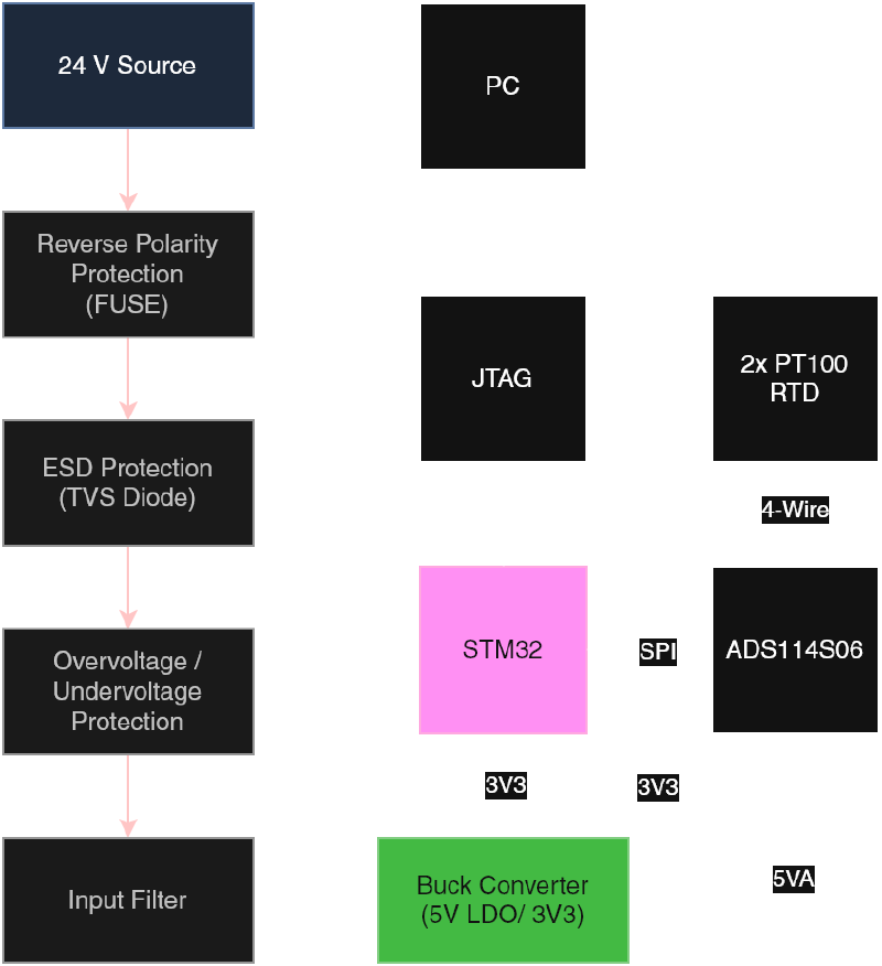
This project is part of the Yellow Jacket Space Program (YJSP) Avionics Department onboarding program. The goal is to design a 2-layer rapid test board that integrates an STM32H573 microcontroller with an ADS114S06 high-precision ADC for four-wire PT100 RTD temperature measurement, along with a complete power regulation chain from a 24V input.
The board serves as a training platform for avionics PCB design skills using Altium Designer and Altium 365, and as a stepping stone into the Hardware-in-the-Loop (HITL) department.
System Architecture#
The design uses a hierarchical schematic structure in Altium Designer, organized into four sheets managed by a top-level sheet:
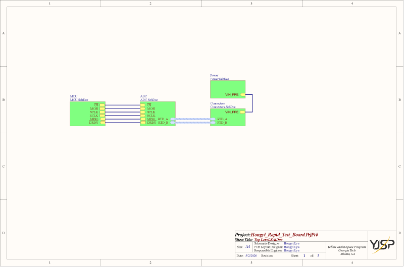
Power (Power.SchDoc) — 24V input with fuse-based overcurrent protection, TVS diode clamping for ESD and overvoltage/reverse polarity protection, GND-to-CGND noise discharge network, and a MAX17503 step-down DC-DC converter providing 3.3V (main rail) and 5V LDO (analog supply). Power-good LED indicators for both 24V and 3.3V rails.
MCU (MCU.SchDoc) — STM32H573RIT6 (ARM Cortex-M33, 250 MHz) with full decoupling network (six 100nF caps on VDD/VSS, 10nF on VDDA, 2.2µF on VCAP), 32 MHz external oscillator (TG2520SMN32.0000M-MCGNNM3), JTAG debug interface via FTSH-107-01-F-DV-K-P-TR 14-pin connector, and SPI bus with series resistors (47Ω) for signal integrity on CS, MOSI, SCLK, ECLK, MISO, and DRDY lines.
ADC (ADC.SchDoc) — ADS114S06IPBS 16-bit delta-sigma ADC with dual power domains (3.3V digital via IOVDD/DVDD, 5V LDO analog via AVDD), separate AGND plane, two four-wire RTD front-end circuits with RC filtering (1kΩ + 10nF/100nF) on each analog input, and a 0Ω resistor (R30) bridging AGND to GND.
Connectors (Connectors.SchDoc) — MOLEX 430450400 4-pin connectors for 24V power input (J1), RTD Channel A (J2), and RTD Channel B (J3). Each RTD connector breaks out IDAC, IDACRTN, RTD_P, and RTD_N signals.
Power Design#
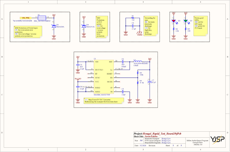
Input Protection#
The 24V input enters through a BEL 0ZCG0150BF2C fuse (F1) for overcurrent protection, then passes through two TVS diodes that serve dual purposes:
D1 (SMAJ26A) — Clamped across the 24V input to GND. Provides overvoltage clamping and reverse polarity error protection. If the input voltage exceeds the breakdown threshold or is applied in reverse, D1 clamps the voltage and the fuse blows, protecting downstream circuitry.
D4 (SMAJ5.0A) — Clamped across the 3V3 rail to GND. Provides ESD protection and overvoltage/reverse polarity error protection specifically for the 3.3V power domain.
Grounding and Noise Discharge#
A grounding network provides static electricity discharge and high-frequency noise filtering between the power ground (GND) and chassis ground (CGND):
R1 (1MΩ) — Connects GND to CGND, providing a controlled path for static electricity discharge while maintaining isolation between the two ground domains at DC.
C2 (4.7nF) — In parallel with R1, provides a low-impedance path for high-frequency noise between GND and CGND, shunting transient energy to the chassis.
Buck Converter (24V → 3.3V)#
The Maxim MAX17503 step-down DC-DC converter directly converts the 24V input to 3.3V output. The schematic follows the datasheet reference design. Key components:
Input stage — C3 (2.2µF, 50V) provides input decoupling. The EN/UVLO pin sets the input undervoltage lockout threshold. A 5V LDO output from pin 12 (VCC) powers the internal gate driver and control logic, with C4 (2.2µF) as the bypass capacitor.
Output stage — L1 (XGL3530-682MEC, 6.8µH) is the power inductor connected to the Lx switching output (pins 17–19). C7 (47µF) is the bulk output capacitor. The output voltage is set to 3.3V by the feedback resistor divider formed by R4 (100kΩ) and R5 (37.4kΩ) on the FB pin.
Auxiliary — C6 (100nF, 50V) is the bootstrap capacitor on the BST pin, required for high-side MOSFET gate drive. C5 (10nF) on the SS pin sets the soft-start ramp time, limiting inrush current at power-up. The RT pin is left unconnected (using the internal default switching frequency). The CF pin capacitor sets the compensation for loop stability.
Power Good Indicators#
Two LEDs provide visual power status indication: D2 (red) lights when 24V input is present, and D3 (green) lights when the 3.3V output is active. R2 (2.2kΩ) and R3 (100Ω) are the respective current-limiting resistors.
MCU: STM32H573RIT6#
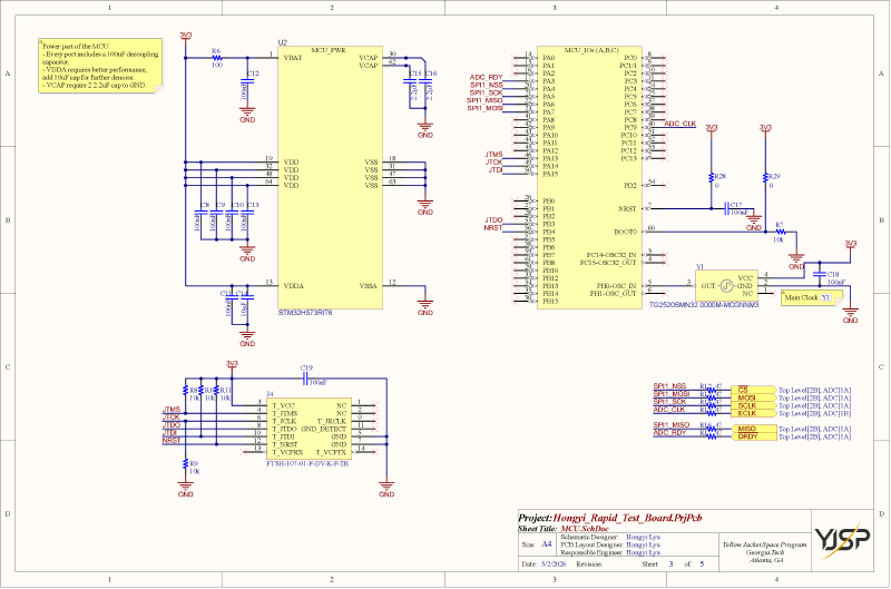
Power and Decoupling#
The MCU power network follows the datasheet recommendations with careful attention to each supply domain. Every VDD pin (pins 19, 32, 48, 64) is bypassed with a 100nF ceramic capacitor (C8–C10, C13) placed as close as possible to the pin. The VDDA analog supply (pin 13) receives additional filtering with both a 100nF cap (C11) and a 10nF cap (C14) to suppress high-frequency noise coupling into the internal ADC reference. The VCAP pins (pins 30, 62) require 2.2µF capacitors (C15, C16) for the internal voltage regulator. VBAT (pin 1) is connected to 3.3V through R6 (100Ω) with C12 (100nF) for backup domain filtering. The MCU_PWR net label is annotated to remind that every port requires its own 100nF decoupling cap and that VDDA benefits from additional 10nF filtering.
Clock Source#
An external 32 MHz crystal oscillator (TG2520SMN32.0000M-MCGNNM3, designated Y1) provides the system clock, connected to PH0-OSC_IN (pin 5) and PH1-OSC_OUT (pin 6). The oscillator is powered from 3.3V (VCC, pin 3) with C18 (100nF) as a bypass capacitor. An additional secondary 32 kHz oscillator input is available on PC14-OSC32_IN (pin 3) and PC15-OSC32_OUT (pin 4) but left unconnected in this design.
Reset and Boot Configuration#
The NRST pin (pin 7) is connected to C17 (100nF) to GND for power-on reset filtering. The BOOT0 pin (pin 60) is tied to GND through R7 (10kΩ), ensuring the MCU boots from internal flash under normal operation.
JTAG Debug Interface#
A full JTAG interface is implemented using a FTSH-107-01-F-DV-K-P-TR 14-pin connector (J4), supporting both JTAG and SWD protocols. The JTMS, JTCK, JTDO, JTDI, and NRST signals are routed through 10kΩ series resistors (R8–R11 for signal lines, R9 for NRST) for ESD protection and signal conditioning. C19 (100nF) provides local decoupling for the T_VCC power pin. The connector also includes GND_DETECT for debugger presence sensing and T_VCPRX/T_VCPTX for trace port functionality.
SPI Bus Interface#
The SPI1 bus signals connecting to the ADS114S06 are routed through 47Ω series resistors (R12–R16) for impedance matching and signal integrity. The signal mapping is:
| MCU Net | Series Resistor | ADC Signal | Direction |
|---|---|---|---|
| SPI1_NSS | R12 (47Ω) | CS | MCU → ADC |
| SPI1_MOSI | R13 (47Ω) | MOSI | MCU → ADC |
| SPI1_SCK | R14 (47Ω) | SCLK | MCU → ADC |
| ADC_CLK | R15 (47Ω) | ECLK | MCU → ADC |
| SPI1_MISO | R16 (47Ω) | MISO | ADC → MCU |
| ADC_RDY | R17 (47Ω) | DRDY | ADC → MCU |
The ADC_CLK line provides an external clock source to the ADS114S06, driven from the MCU’s PC9 pin (pin 40). Two pull-up resistors R28 and R29 (0Ω, placeholder for value selection) connect the 3.3V rail to the ADC SPI interface for optional pull-up configuration. PD2 (pin 54) is marked as an available spare GPIO.
ADC: ADS114S06IPBS#
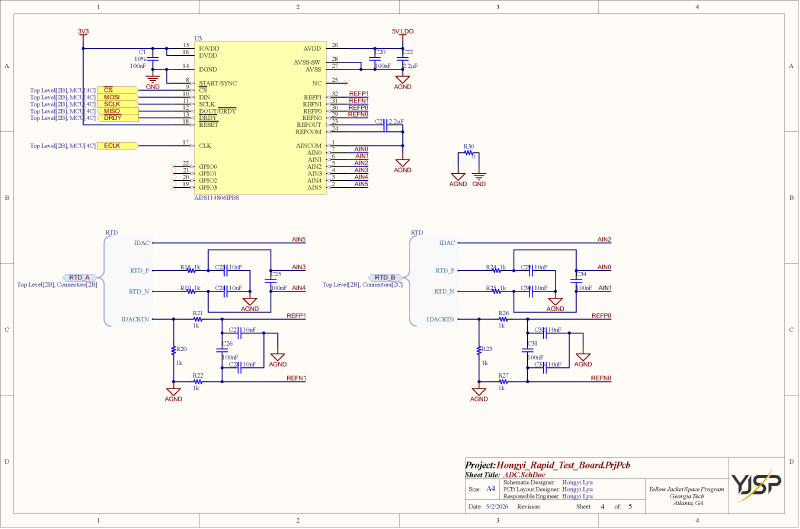
Power Domains#
The ADS114S06 operates with split power domains to isolate digital noise from the sensitive analog front-end. IOVDD (pin 15) and DVDD (pin 16) are powered from the 3.3V digital rail with C1 (100nF, 10% tolerance) as the local bypass capacitor. DGND (pin 14) connects to the digital GND plane. The analog supply AVDD (pin 26) is powered from the MAX17503’s 5V LDO output, bypassed by C20 (100nF) and C22 (2.2µF). AVSS (pins 27–28) connects to the dedicated AGND plane, which is bridged to GND through a single-point connection via R30 (0Ω). This star-ground topology prevents digital return currents from flowing through the analog ground plane.
SPI and Control Interface#
The digital interface signals (CS, MOSI, SCLK, MISO, DRDY, ECLK) arrive from the MCU sheet through hierarchical sheet connectors, each pre-conditioned by 47Ω series resistors on the MCU side. The START/SYNC pin (pin 8) is directly tied, and the RESET pin (pin 18) is directly connected for MCU-controlled reset. The DRDY output (pin 13) active-low interrupt, directly active. Pin 12 (DOUT/DRDY) provides multiplexed data output and ready signaling on a single pin.
Reference Configuration#
The ADC uses external ratiometric referencing for the RTD measurements. Two independent reference pairs are used for the two RTD channels: REFP1/REFN1 (pins 32/31) for RTD Channel A, and REFP0/REFN0 (pins 30/29) for RTD Channel B. The REFOUT (pin 23) and REFCOM (pin 24) internal reference outputs are bypassed with C21 (2.2µF) but the primary measurement references are derived from the IDAC excitation current flowing through the reference resistors in the RTD front-end circuits.
Analog Input Channels and RTD Front-End#
Each RTD channel uses a dedicated analog front-end circuit with RC filtering on every signal path to reject high-frequency interference before it reaches the ADC inputs.
Channel A (RTD_A) uses AIN3/AIN4 for voltage sensing and AIN5 for IDAC excitation, with REFP1/REFN1 as the reference pair:
| Signal | ADC Pin | Filter | Function |
|---|---|---|---|
| RTD_P → AIN3 | pin 4 | R18 (1kΩ) + C24 (10nF) + C25 (100nF) | Positive voltage sense |
| RTD_N → AIN4 | pin 3 | R19 (1kΩ) + C23 (10nF) | Negative voltage sense |
| IDAC → AIN5 | pin 2 | — | Excitation current output |
| IDACRTN → REFP1 | R21 (1kΩ) + C27 (10nF) | Excitation current return / Reference+ | |
| AGND → REFN1 | R22 (1kΩ) + C26 (100nF) + C28 (10nF) | Reference− |
Channel B (RTD_B) uses AIN0/AIN1 for voltage sensing and AIN2 for IDAC excitation, with REFP0/REFN0 as the reference pair:
| Signal | ADC Pin | Filter | Function |
|---|---|---|---|
| RTD_P → AIN0 | pin 7 | R24 (1kΩ) + C29 (10nF) + C34 (100nF) | Positive voltage sense |
| RTD_N → AIN1 | pin 6 | R25 (1kΩ) + C30 (10nF) | Negative voltage sense |
| IDAC → AIN2 | pin 5 | — | Excitation current output |
| IDACRTN → REFP0 | R26 (1kΩ) + C32 (10nF) | Excitation current return / Reference+ | |
| AGND → REFN0 | R27 (1kΩ) + C31 (100nF) + C33 (10nF) | Reference− |
The R20/R23 (1kΩ) resistors in the IDAC return paths limit current and provide additional filtering nodes. All analog ground connections on the front-end circuits connect to AGND, maintaining isolation from the digital GND domain.
Connectors#
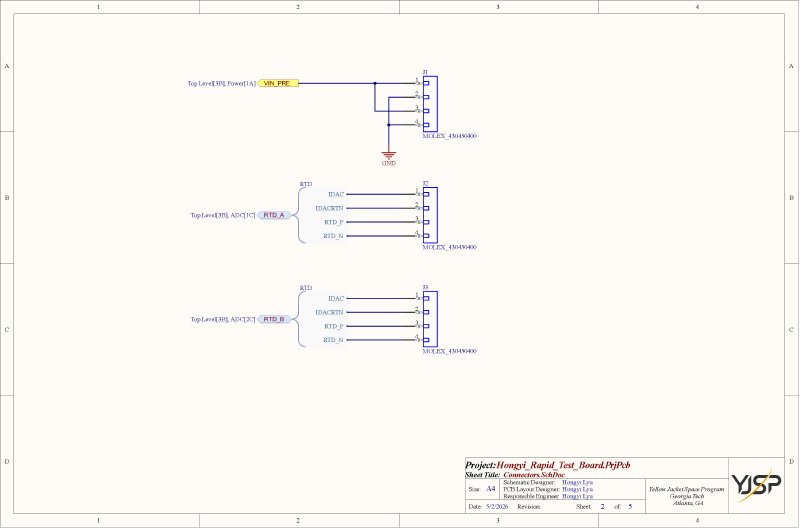
Three MOLEX 430450400 4-pin connectors provide the external interfaces:
J1 (Power Input) — Receives the 24V supply through the VIN_PRE net from the Power sheet. Pin 1 carries VIN_PRE, pins 2–4 are paralleled for ground return, providing a robust low-impedance power connection.
J2 (RTD Channel A) — Breaks out the four-wire RTD_A interface. The pinout maps IDAC (pin 1), IDACRTN (pin 2), RTD_P (pin 3), and RTD_N (pin 4), matching standard four-wire RTD cable assemblies.
J3 (RTD Channel B) — Identical pinout to J2 for RTD_B, enabling the second independent temperature measurement channel.
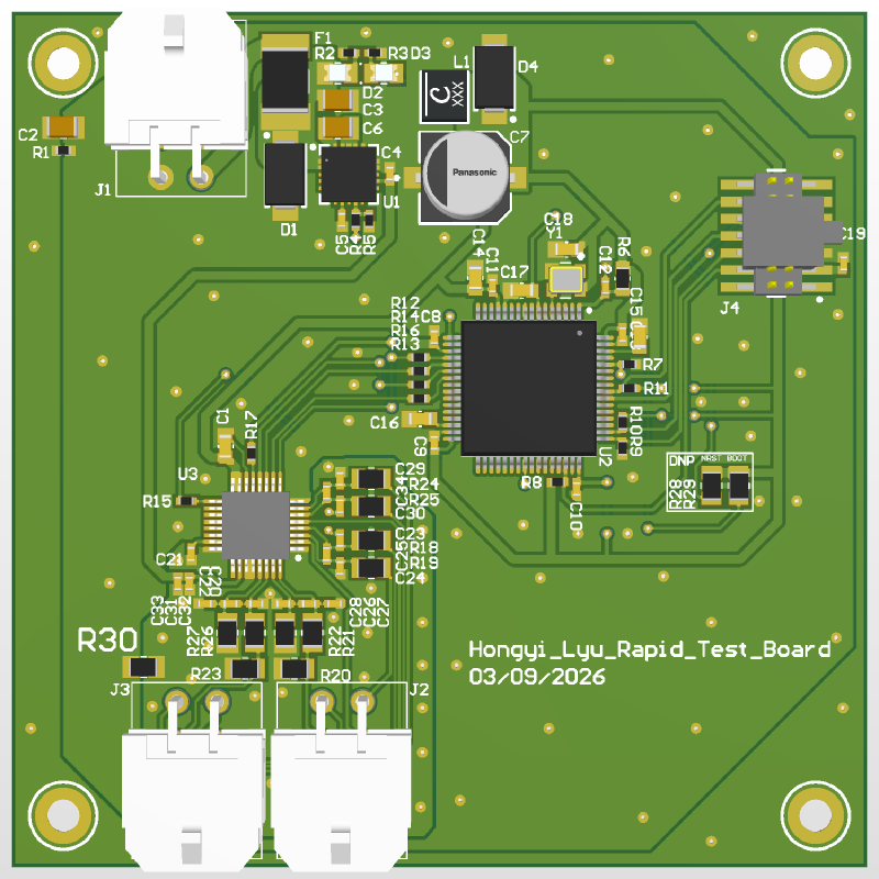
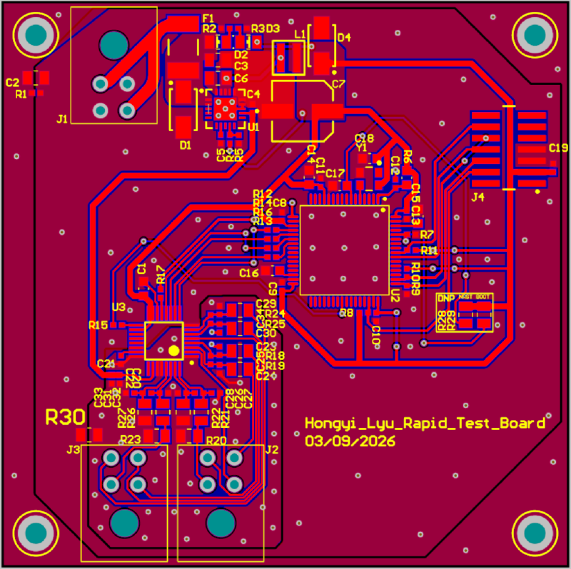
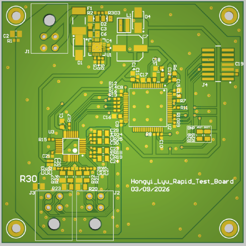
PCB Design#
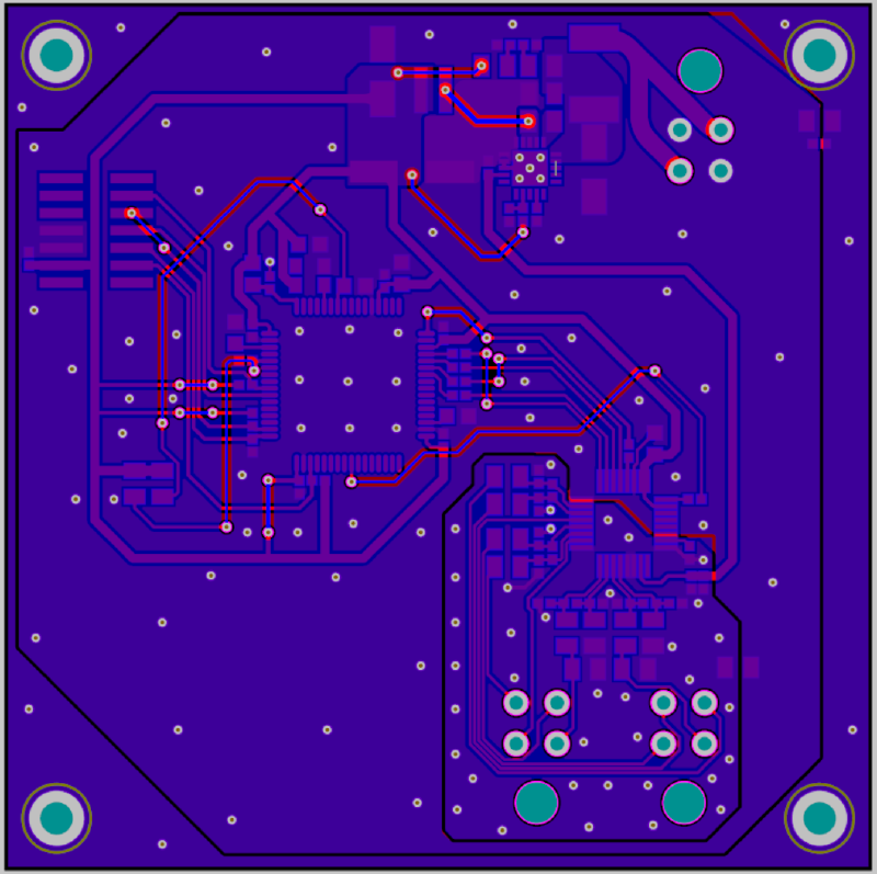
Layer Stackup#
The board is a 2-layer design in order to reduce cost (and also practice wiring on limited dimensions).
| Layer | Function |
|---|---|
| Top | Signal routing, component placement |
| Bottom | Ground plane, secondary routing |
A solid ground plane on the bottom layer provides low-impedance return paths and reduces electromagnetic interference.
Layout Strategy#
The PCB layout follows a modular placement strategy aligned with the signal flow:
- Power input and protection — Top-left side of the board, near the 24V connector
- Buck converter and Power — Tight layout with wide traces between IC, inductor, and capacitors to minimize switching loop area
- MCU — Center of the board, with decoupling capacitors placed directly adjacent to each VDD pin
- ADC — Near the MCU to keep SPI traces short, with analog input traces routed away from digital switching noise. AGND plane isolated from digital GND with single-point 0Ω bridge
- Sensor connectors — Board edge for easy cable access
- SWD/JTAG header — Board edge for programming access
Design Rules#
| Parameter | Value |
|---|---|
| Minimum trace width | 0.203mm (8mil) |
| Minimum clearance | 0.254mm (10mil) |
| Via hole size | 0.3mm |
| Via pad size | 0.6mm |
| Power trace width | ≥0.5mm (20mil) |
ERC and Design Review#
The schematic passed Electrical Rules Check (ERC) with all errors resolved. Key issues encountered during the review process included:
- Unconnected power pins on the MCU requiring explicit no-connect markers
- Net label mismatches between hierarchical sheets
- Missing decoupling capacitors flagged by team reviewers
The design went through multiple team review iterations on Altium 365, incorporating feedback on component selection, layout spacing, and trace routing.
Tools & Skills#
What I Learned#
This onboarding project was my transition from LCEDA (EasyEDA) to the Altium Designer ecosystem. The biggest adjustments were the hierarchical schematic structure (four sheets managed by a top-level sheet with inter-sheet connectors), the netlist synchronization workflow (ECO process), manual symbol-footprint-3D model association for each component, and the more complex layer management system.
Designing a complete power chain from 24V down to 3.3V using the MAX17503 switching regulator — including fuse protection, TVS clamping, and GND/CGND isolation — was a significant step up from my previous projects, which typically started from USB 5V or battery power. Learning to read and implement a datasheet reference design (selecting feedback resistors for target output voltage, sizing the bootstrap and soft-start capacitors, choosing the power inductor) was a core skill I developed through this project.
The analog design aspects were equally valuable. Implementing split power domains (3.3V digital / 5V LDO analog) for the ADS114S06, designing the AGND-to-GND single-point star ground topology with a 0Ω bridge resistor, and adding 47Ω series resistors on every SPI line for signal integrity taught me how precision analog circuits require fundamentally different design practices than pure digital systems. Understanding the four-wire RTD measurement architecture — how IDAC excitation, ratiometric referencing, and RC input filtering work together to achieve high-accuracy temperature measurement — deepened my appreciation for the interplay between circuit design and measurement theory.
Next Steps#
Following completion of this onboarding board, I entered the YJSP HITL department, where the scope expanded to include:
- 4-layer PCB design with dedicated power and ground planes
- LMR36015-based 24V→6V buck converter with INA228 current monitoring
- PCF8575 GPIO expansion driving ULN2803A relay arrays for valve control
- Multi-rail power distribution with separated AGND/GND/CGND domains and ferrite bead isolation
Reference#
There are no articles to list here yet.